IBM has unveiled its latest chip based on 5nm technology, in collaboration with Samsung and Global Foundries! The most exciting thing about this chip is that it was fabricated based on a new transistor technology called
Gate-All-Around transistor (GAA). This is the first ever chip fabricated with these transistors! The normal transistor fabrication uses Ultra Violet radiation for lithography but the GAA transistors need extreme UV (EUV) lithography and IBM has succeeded in this fabrication!
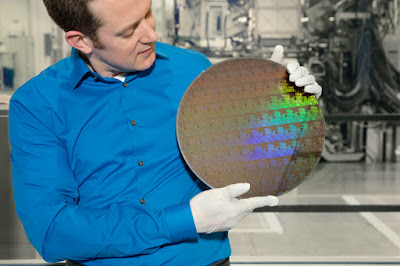 |
| Wafer of 5nm chip |
Transistor chronology in IC fabrication:
Initially, Diodes, followed by Bipolar Junction Transistors (BJTs), followed by MOSFETs (Metal Oxide Semiconductor Field Effect Transistor) has been the hierarchy of transistor-level IC fabrication. MOSFETs have ruled the industry for a long period. But, due to the limitations of MOSFET, FinFET has been introduced and Trigate FinFET was also introduced in parallel. But, beyond all these transistor technologies, the GAAFET transistors came into picture for the world's first 5nm chip. Researches suggest that the GAAFETs are completely functional upto 3nm with EUV lithography. But, no one knows what happens if the channel length still shrinks!
Geometric paradigms in IC fabrication:
2D and 3D are the two paradigms in IC fabrication. As the channel length kept on shrinking, 2D ICs were unable to inculcate required functionalities into single chip. Hence, 3D ICs were opted. However, the success rate of 3D ICs is very less compared to that of the 2D ICs. On the other hand, chips with FinFET transistors were also fabricated in both the paradigms, which does not result in a notable improvement.
Abiding all the limitations in different technologies, GAAFETs were able to succeed the channel length limitations. There are different ways of fabricating an IC with GAAFETs but, IBM's chip was fabricated with the horizontal devices. If a FinFET is rotated 90 degrees then, it forms a vertical fin and the channel becomes horizontal fin. In other words, the fin becomes a silicon nanowire stretched between the source and drain terminals. Here is the technical data related to this fabrication.
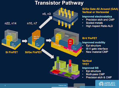 |
| Pathway of transistor fabrication |
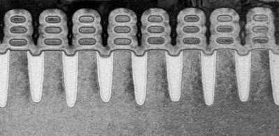 |
| 5nm nanosheets in GAAFETs |
Fabrication details of GAAFETs:
In this process of fabrication, layers of Si and Si-Ge are laid alternatively. Later, the Si-Ge layers are etched out so that the Si layers alone stay back, which are called nano sheets. Etching of Si-Ge layers is achieved through a new etching technique called Atomic layer etching. The gaps formed by the etching of Si-Ge layers is deposited with high dielectric gate material, with a new technique called Atomic layer deposition. Note that these operations are performed at the atomic level and hence the prefix "atomic".
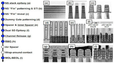 |
| Stages of GAAFET fabrication |
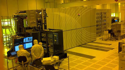 |
| ASML EVU machine for etching the 5nm chips |
 |
| Wafer washing machines |
There are many complexities in the patterns of deposition and etching of different layers during fabrications. But, GAAFET manufacturing draws advantage in these pattern complexity. The previous lithographic process used UV radiation of 193nm wavelength but with Extreme UV, the wavelength has narrowed down to 13.5nm, which is a great advantage of GAAFETs over conventional FETs and FinFETs. This reduces the number of stages for patterning compounded.
Metrics of performance compared:
When compared to 10nm MOSFET/FinFET chips, the new 5nm chip offers 40% improved performance and 75% reduction in power consumption! IBM claims that 30 billion transistors can be embedded on to a chip of 50 sq.mm area! This size can be perceived to the size of our finger nail. On the other hand, the time taken to manufacture chips using this transistor technology is very less when compared to the conventional transistors. Researchers say that though FinFETs are favourable to work when shrinked upto 5nm, it is better to opt for the GAAFETs, in order to save the time invested in fabrication of a chip.
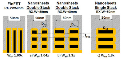 |
| Gate size GAAFET vs FinFET |
The sad end is that IBM has not revealed the image of the chip, neither the commercial availability of the chip. It is still saddening that there is no word about the applications of this exciting and revolutionary technology.


0 comments:
Post a Comment