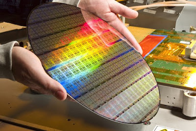
Chip technology has now reached a saturation stage; the pace of Moore's law has also slowed down. This is due to the limitations of MOSFET technology. The technology has reached a stage where the MOSFETs cannot serve the ON/OFF switching effectively. In order to overcome these limitations, IBM has adopted a new transistor technology called Gate-All-Around transistors (GAAs), that can fabricate chips even with 5nm technology.
The firms like TSMC and Samsung have opted for 10nm technology immediately after 14nm technology, which is not the conventional trend of adopting the next chip fabrication technology. For example, 180nm technology was followed by 90nm technology, followed by 45nm and 22nm technologies. As 14nm technology is adopted after 22nm technology instead of 11nm, the firms mentioned undertook 10nm technology instead of 7nm technology.
GlobalFoundries is one of the world's leading semiconductor manufacturers, based in the US. Unlike TSMC and Samsung, GlobalFoundries has opted for 7nm after its 14nm technology chips, following the conventional "halving" principle of technology upgrading. With the 7nm technology, GlobalFoundries is going to launch its own kind of fabrication process.
Image source: Anandtech
GlobalFoundries is going to implement the Deep Ultra Violet lithographic process in its new fabrication. With this adoption, the performance is expected to be improved and power consumption to be reduced, in comparison with the 10nm technology chips. The following is the comparison between the three generations of 7nm chips from GlobalFoundries.
The firms like TSMC and Samsung have opted for 10nm technology immediately after 14nm technology, which is not the conventional trend of adopting the next chip fabrication technology. For example, 180nm technology was followed by 90nm technology, followed by 45nm and 22nm technologies. As 14nm technology is adopted after 22nm technology instead of 11nm, the firms mentioned undertook 10nm technology instead of 7nm technology.
GlobalFoundries is one of the world's leading semiconductor manufacturers, based in the US. Unlike TSMC and Samsung, GlobalFoundries has opted for 7nm after its 14nm technology chips, following the conventional "halving" principle of technology upgrading. With the 7nm technology, GlobalFoundries is going to launch its own kind of fabrication process.
 |
| GlobalFoundries 7LP Platform Process and Features |
GlobalFoundries is going to implement the Deep Ultra Violet lithographic process in its new fabrication. With this adoption, the performance is expected to be improved and power consumption to be reduced, in comparison with the 10nm technology chips. The following is the comparison between the three generations of 7nm chips from GlobalFoundries.
 |
| GlobalFoundries 7LP Platform |
Read more: MediaTek latest SoCs


0 comments:
Post a Comment